Multibeam Optical Sensor (MOS) - A Laser Based Thin Film Growth Monitor
From www.k-space.com
by Charles Taylor, Darryl Barlett, Eric Chasen, and Jerry Floro
|
|
|
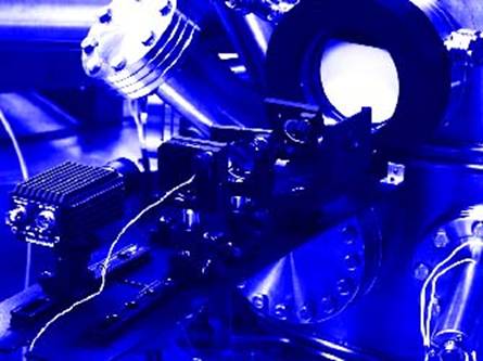
Figure 1. Multibeam optical sensor mounted on a commercial
thin-film deposition system. |
The
Multi-beam Optical Sensor (MOS) was developed jointly by k-Space Associates
(Ann Arbor, MI) and Sandia National Laboratory to directly measure film stress
and thickness in real-time during fabrication (Figure 1). Understanding and
controlling stress in thin films are critical for achieving the desired
optical, electronic, and mechanical properties. Many of today’s high
performance devices rely on "built-in" strain within the individual
layers for tailoring specific characteristics. Controlling the degree of strain
poses a significant challenge. On the other hand, unwanted changes in strain
can be introduced at any stage of the fabrication process and may lead to
degradation in device performance as well as failure of interconnects and
delamination of films.
BACKGROUND
Deposition
of thin film materials for electronic and optoelectronic devices requires
precise control of the deposition process. Typically, information is obtained
about the thin-film growth from a limited assortment of sensors. These sensors
measure process parameters, such as gas flow rate, chamber pressure, and
evaporation-source temperature. The parameters are predetermined using
empirical results to produce a film with the desired thickness, microstructure,
and electronic and optical properties. The actual film properties or device
characteristics are usually measured after the deposition is completed.
Improvements
in both process sensors and control systems have lead to very stable operation
during the time required to fabricate a thin-film device. The problems lie in
the variations that occur on a day-to-day or weekly basis. Such variations in
the process often lead to unpredictable changes in deposition rate or film
composition, which can drastically alter the film properties. Calibration runs,
which involve costly downtime, must be performed regularly to ensure and
maintain device specifications.
Recent
developmental efforts in process control have focused on in situ sensors to
directly measure film properties during deposition. Ideally, such sensors would
provide complete information about the state of the film and substrate at any
instant during fabrication. This information could be used to continuously adjust
process parameters to optimize film properties and correct for unexpected
variations as they occur. Optical-measurement techniques are the natural choice
for such sensors because they are noninvasive, can be mounted outside the
deposition chamber, and are typically insensitive to the level of stray
electric and magnetic fields associated with thin-film-fabrication equipment.
Furthermore, many commercial thin-film-deposition processes involve
high-pressure, chemically reactive environments, which make optical techniques
the only viable option for in situ sensors.
The
principles underlying the MOS technique are simple. Basically, a thin film
under stress will induce a curvature k = 1/R, in the underlying substrate. Here
R is the radius of curvature on the surface of the thin film. The film stress
in turn can be calculated from k by a simple equation, originally developed by
Stoney in 1909, that requires only knowledge of the film and substrate
thickness, as well as the elastic modulus of the substrate.
Thus
the challenge of the MOS technique is to accurately detect curvature in the
substrate with sufficient resolution to measure the amount of stress typically
found in thin films. For very thin films, on the order of tens of angstroms,
this resolution may require detecting a radius of curvature as large as 10 to
20 km.
Researchers
have devised various experimental approaches to measure the curvature of a
surface. We will concentrate on techniques that use deflection of a beam of
light from the sample surface. Consider, first, a perfectly flat sample
surface. If one moves a laser beam across the surface at a constant angle, then
the angle of deflection will be the same everywhere on the surface. With a
curved surface, then the amount of deflection will change as the beam is
transverses the sample.
|
|
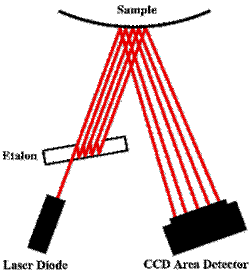
Figure 2. An etalon placed at
an angle to a laser beam generates a linear array of parallel beams. These
beams reflect off the sample surface and are directly imaged by a CCD
detector. |
In
one such technique, a rotating mirror scans a laser across the sample without
changing the angle of incidence. A position-sensitive detector (PSD) measures
the deflection of the beam during scanning. This technique is currently used in
bench-top measurement systems and even on some fabrication lines, but only as a
postprocess diagnostic. The primary drawbacks of this approach lie in the need
for precise alignment of the sample with respect to the focusing optics, and
the use of a rotating mirror. Precise alignment of the sample is not possible
in most deposition systems, and laser scanning is much more sensitive to
vibration than a multibeam, stationary optic approach. A simple alternative
uses a beam splitter to produce two parallel beams whose deflections are
measured independently with position-sensitive detectors. Although extremely
robust and offering good curvature resolution, this approach is limited to
measuring only two positions on s sample.
MULTIBEAM
OPTICAL SENSOR
The
Multibeam Optical Sensor uses a variation of this technique as well as other
features that simplify its use for in situ diagnostics (Figure 2). An etalon,
with highly reflective dielectric coatings on each side, is placed at an angle
to a laser beam. The incidence angle of the laser leads to multiple internal
reflections within the etalon, which generates a linear array of parallel
beams. These beams then pass through a second rotated etalon to produce a
2-dimensional array of beams. The number and spacing of these beams can be
controlled by the rotation angle of each etalon. The low power (uW) array of
parallel beams is then reflected from the sample surface and directly imaged
with a charge-coupled device (CCD) camera.
|
|
Figure 3. Superposition of a laser spot array imaged from a silicon
surface before (red) and after (blue) the wafer has been stressed; maximum
deflection of the surface is 5 um. |
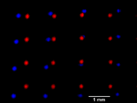
Figure
3 shows an example of the laser-array image measured by the CCD detector. The
array was first reflected from an unstressed 2-in.-diameter silicon wafer. Then
a force applied to the back of the wafer stressed it non-uniformly. The induced
curvature caused the individual beams to reflect to slightly different
positions on the detector. The relative change in spacing of all the spots was
measured simultaneously by the CCD detector, and the data was then converted to
represent the surface displacement or radius of curvature (Figure 4).
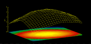
|
Figure 4. Surface
displacement of a silicon wafer calculated from the changes in the laser spot
array shown in Figure 3. |
|
The
use of a laser-beam array and CCD detector provides several benefits for
in-situ measurement. The primary advantage is that the optics are simple and
stationary, requiring only minimal alignment during initial setup. The ability
to directly image and view the entire reflected laser array greatly simplifies
use and alignment compared with other position sensitive detectors.
Simultaneous detection of the array makes the measurement inherently less
sensitive to sample vibration compared with scanning-mirror systems. Since all
the laser spots move together at the same frequency, movement or tilt is not
detected as a change of curvature. Critical to the measurement is the use of a
high- resolution CCD array that enables highly accurate determination of the
spot positions. Through the use of simple image-processing and data-analysis
algorithms, MOS can easily detect micron-size changes in spot position. This
translates to a curvature detection of 10 to 20 km in the fabrication
environment. Such a level of sensitivity enables the system to detect single
monolayers deposited on the substrate surface. By monitoring the entire array
of beams, two-dimensional, spatially varying curvature and stress profiles can
be obtained with enough speed necessary for real-time measurement and process
control.
Two
major issues needed to be solved before the MOS technique could be applied as a
routine diagnostic and control sensor. The first involved making the technique
available to industrial deposition chambers, where the sample is continuously
rotating to improve material uniformity. By placing an optical shaft encoder on
the rotation stage, the CCD detector and image-acquisition electronics are
triggered by the encoder to acquire an image at a preset rotation angle(s). In
addition, the user can select the speed of the CCD’s electronic shutter. Short
shutter times (typically 1/5,000 s) yield images that are acquired over a very
small rotation angle, eliminating image "blurring." In this matter,
extremely stable stress and thickness data are obtained during rotation.
A
second issue involves the changing reflectivity of the sample, which is a
concern for all optical- based sensors. In many applications, thin films are
deposited on substrates, such as silicon or gallium arsenide, which have a very
different reflectance from that of the films being deposited. For example,
depositing copper on a semiconductor substrate such as silicon will cause the
reflectivity of the sample to increase rapidly during the first few seconds of
the process. Such a change will increase the intensity of the laser spots and
can easily saturate the CCD detector. When this occurs, the accuracy in
determining the position of each spot on the CCD is reduced, leading to large
errors in the measured stress.
This
problem was solved by using a controllable diode laser. Technological advances
have enabled the production of robust solid-state diode lasers operating in the
visible spectrum. The output power of the laser is stable and adjustable,
yielding rapid and accurate feed back control. Through additional image
processing, the intensities of each reflected laser spot on the CCD detector
are used as feedback control to the laser-diode controller. The intensity of
the reflected array is monitored continuously and adjusted to optimize the
signal at the detector.
Monitoring
the intensity of the reflected laser-array can provide a wealth of additional
information about the film. If the films index of refraction differs from that
of the underlying substrate, then the reflected laser intensity will oscillate
as the film thickness increases. The shape of the oscillations can be fitted
very accurately to a model for thin-film interference of coherent monochromatic
light. The fitting algorithm used is based on a "virtual interface"
model that can easily handle a multilayer-film structure without precise
knowledge of the positions of the film interfaces. This algorithm provides a
fully automated procedure for extracting the film thickness and
high-temperature optical constants, during deposition, with no prior knowledge
other than the starting reflectance of the substrate. Although other accurate,
in situ methods can measure optical properties and thickness of thin films,
such as spectroscopic ellipsometry and spectroscopic reflectance, the intensity
information provided by the single-wavelength laser array is sufficient for
most applications and is simply serves as an added benefit to the MOS
technique.
A
number of facilities- including Motorola, Lockheed Martin, and the University
of Michigan- are using the new sensor technology to monitor the deposition of
compound semiconductors, oxides, nitrides, and diamondlike coatings by a
variety of methods such as chemical-vapor deposition (CVD), sputtering, and
molecular-beam epitaxy. Sandia National Laboratory has several MOS systems in
use. One monitors the stress of gallium nitride films grown on gallium
arsenide. The sample rotates at 1,200 rpm, and an optical shaft encoder
triggers one image acquisition per revolution, yielding near real-time stress
measurement. The stress value can be relayed as a voltage signal to the
CVD-control system, yielding a feedback mechanism for controlling strain and
constituent composition.
This
article is in the March '98 issue of the The
Industrial Physicist