Research Highlight
|
|
|
|
|
|
|
|
|
|
|
Dimer on Si (001) surface Molecular dynamics simulation of Si (001) surface revealed the characteristics of surface dimers. Depending on the vicinal direction, dimer would have different interaction with the vicinal step. Left is the SMT microstructure of Si (001) surface. Center snap shot shows that the dimer are aligned alternatively for each terrace when the vicinal direction is [110]. On the [100] vicinal direction surface (right), all steps have identical relationship with the dimer line of each surface. (2007. 6. 15) |
Cu doped GaN, as a novel DMS materials Ab initio calculation of transition metal doped GaN showed that Cu is promising dopant for the room temperature ferromagnetic semiconductor. By Cu implantation into GaN, this prediction was confirmed experimentally by Dr. J. H. Song at KIST. (related publication)(2007. 6. 15) |
||
|
|
|||
|
|
|
|
|
|
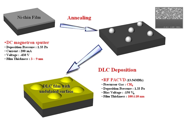
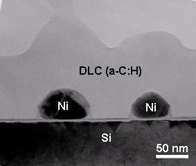
Environmental Dependence of Nano-undulated Surface As expected from the tribochemical interaction on the nanoundulated surface, humidity dependence of the friction was much reduced as the roughness of the surface increased in nanometer scale. Nanoundulated DLC surface was prepared using nano-sized metal dots on Si wafer as the substrate (left). Difference in the friction coefficient for various relative humidity became smaller as the roughness increased. (2007. 6. 15) |
Structure Evolution of Al Thin Film on Cu substrate Atomic scale understanding of the structure evolution becomes very important in nano-devices, such as magnetic spin valve. Al deposition behavior was investigated on Cu substrate by molecular dynamics simulation. These results provide an insight for understanding the structure evolution in Al-Cu system. (2007. 6. 15) |
||
|
|
|||
|
|
|
|
|
|
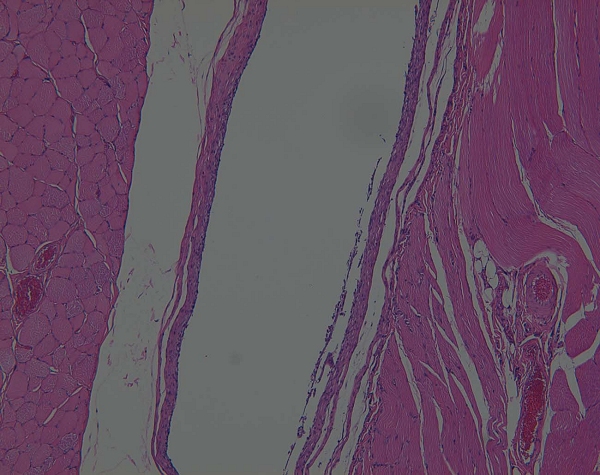
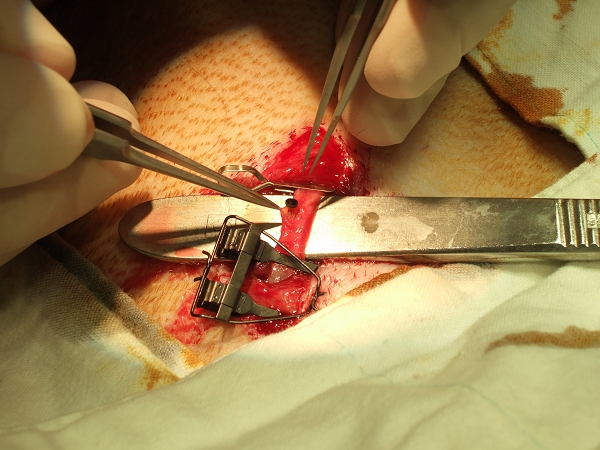
Bio and Hemocompatibility Test (In Vivo) In vivo biocompatibility and hemocompatibility tests are in progress with researchers at Asan Hospital in Seoul. Biocompatibility of Si-DLC coating nitinol coupons was tested in thigh muscle of white rat. Left picture shows the fibrosis tissue after 4 weeks of implantation of Si-DLC coating nitinol. Small nitinol coupons with various DLC coatings are inserted into femoral artery of dog (right picture). Sample surface is inspected after 6 weeks in the artery. Micro-surgery is essential for this test. (2007. 6. 15) |
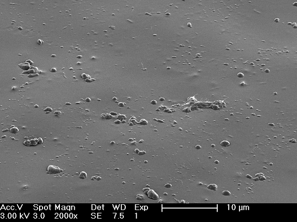
Platelet on the Surface Modified Si-DLC Coating Adhesion and activation of the platelet are significantly suppressed by oxygen and nitrogen plasma treatment of Si-DLC surface. Left SEM picture shows that most platelets are activated on the as-deposited Si-DLC surface. On the other hand, much smaller number of platelets are observed on the nitrogen plasma treated surface. (right SEM picture) We are collaborating with Prof. T. Hasebe at Tachikawa hospital of Keio University and Prof. A. Kamijo at University of Tokyo Hospital. (2007. 6. 15) |
||
|
|
|||
|
|
|
||
|
Superhydrophobic Surface By combining nano-scale surface roughening with a hydrophobic a-C:H:Si:O coating, we generated the super-hydrophobic surface with very low wetting angle hysteresis. Dual structured surface which mimics the lotus leaf was prepared by using nano-sized metal dots as mask of the plasma etching process. The dual structure surface is super-hydrophobic of the wetting angle 160° with the wetting angle hysteresis less than 5°. (Collaborated with Dr. Klaus Bewilogua at Frounhofer Institute, Braunshweig, Germany) (related publication) (2006. 7. 26) |
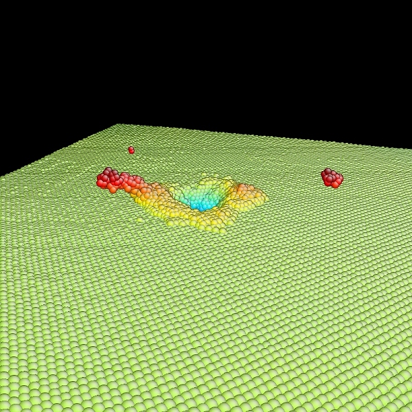
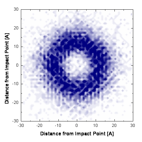
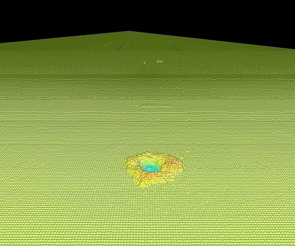
Surface Structure Evolution by High Energy Ion Bombardment Molecular dynamics simulation of high energy Ar ion bombardment on Au surface revealed that the surface atoms are significantly displaced from their original position. Left figure is a snapshot of the Au surface after 10keV Ar ion bombardment. By repeating this simulation, we obtained statistical distribution of the displaced surface atoms as shown in the center figure. This distribution seems to be related with the surface characteristics of the sputtered surface (right figure). More simulations are in progress. (2007. 6. 15) |
||
|
|
|||
|
|
|
|
|
|
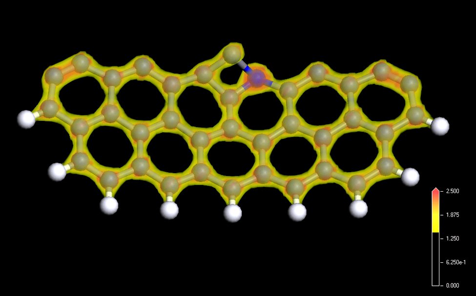
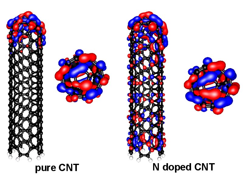
Nitrogen doped CNTs Nitrogen incorporation significnatly enhances both the growth rate of CNT and the field emission behavior. ab-initio calculation revealed the underlying physical mechanism based on the electronic structure of nitrogen atoms embedded in the carbon networks. Nitrogen doping increased the emission current owing to a shift in the energy level of a localized state to the Fermi level, and the creation of coupled states that have characteristics of both localized and extended states. (Collaborated with Prof. Seungwu Han at Ehwa Womans University.) (related publication) (2006. 7. 24) |
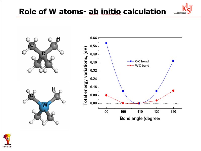
Ab initio study of Me-C bonds The electronic structure of a metal-incorporated carbon system reveals that the bond characteristics between metal and carbon strongly depend on the incorporated metal elements. Incorporation of Mo and Ag significantly reduces the strength and directionality of the bonds while keeping the sp3 structure, which reduces the residual stress without a significant degradation of the mechanical properties. Al incorporation prefers the formation of sp2–like two-dimensional structures, which would significantly decrease both the residual stress and the mechanical properties. (related publication) (2006. 7. 25) |
||
|
|
|||
|
|
|
|
|
|
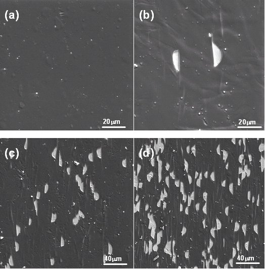
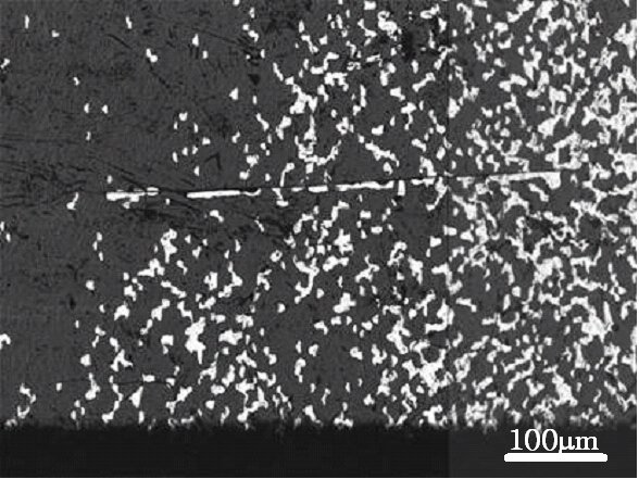
Fracture Behavior of DLC film during Tensile Test Fracture and spallation of the coating occurred during micro-tensile test of the film/substrate composite. As the tensile deformation proceeded, cracks of the film appeared in the perpendicular direction to the tensile axis. Further deformation resulting in the local necking with shear band of 55o inclined to the tensile axis, induced the spallation of the film, which was initiated at the cracks of the film, and was aligned along the slip directions. (collaborated with Prof. Rizhi Wang at Univ. British Columbia, Canada) (related publication) (2006. 7. 24) |
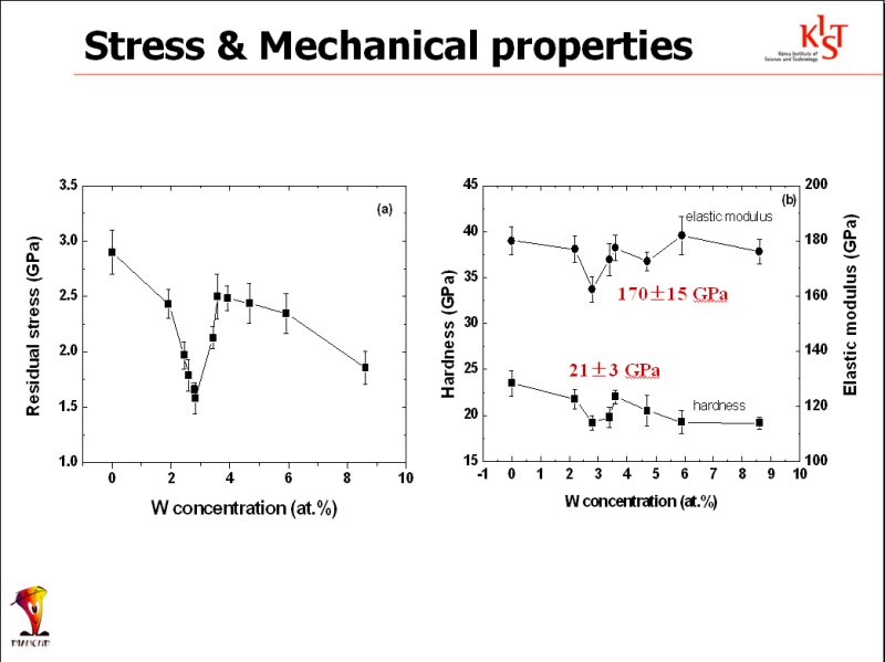
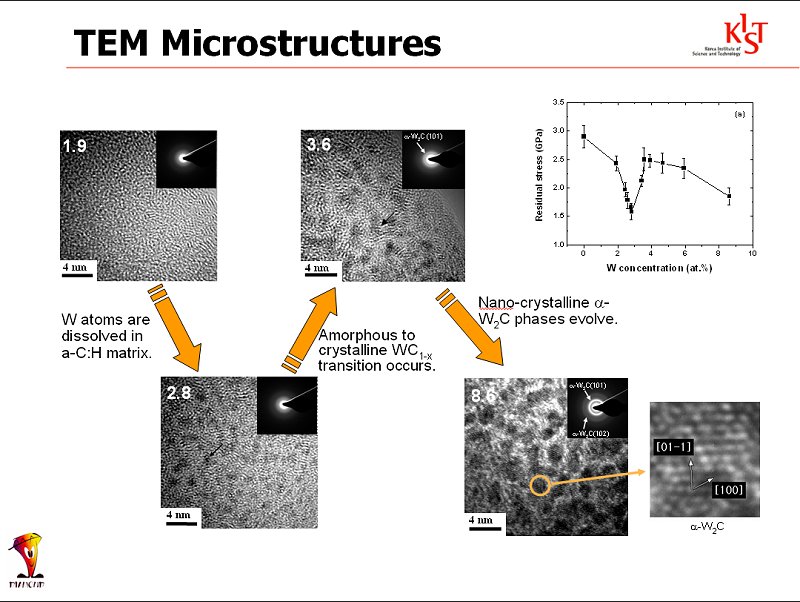
W incorporated DLC Films Unusual stress behavior was observed in W-incorporated DLC prepared by a hybrid process composed of ion beam deposition and magnetron sputtering. High-resolution TEM analysis and first-principle calculations show that the reduced directionality of the W-C bonds in the W incorporated amorphous carbon matrix relaxes the stress caused by the distorted bonds.(related publication) (2006. 7. 24) |
||
|
|
|||
|
|
|
|
|
|
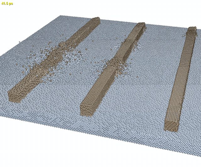
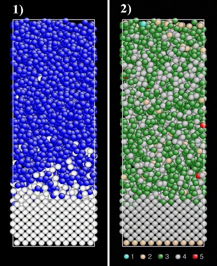
Massive MD Simulation Massive MD simulation using the parallel computing technology will provide the more realistic insights. Based on the LAMMPS developed by Dr. Steven Plimpton at Sandia National Lab. USA, we are customizing the code for thin film deposition of metals and covalent materials. MD movies of 50 million atoms was demonstrated at the end of 2006 (right). Figures above show the intermixing behavior of the Ge nanowire on Si (100) surface at 700oC (left) and the Au surface bombarded by a 10 KeVAr ion (right). (2007. 6. 15) |
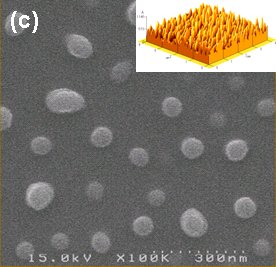
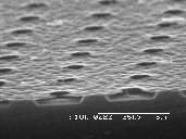
Nano-undulated DLC Film a-C:H coating by r.f.-PACVD on the Si substrate with nano-sized Ni dots resulted in the nanoundulated DLC films of the surface roughness ranging from 0.6 to 13.7 nm. Friction and wear behaviors show that the tribochemical reaction is much suppressed on the nanoundualted surface. (related publication) (2006. 7. 24) |
||
|
|
|||
|
|
|
|
|
|
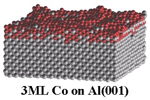
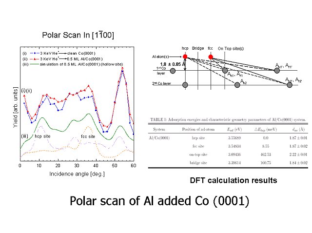
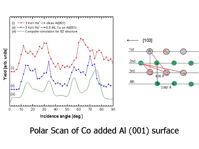
Interface structure in atomic scale Interfacial structure evolution during thin film deposition is now being investigated in atomic scale. Molecular dynamics shows asymmetry in atomic scale intermixing in many metal thin film systems. Al atoms deposited on Co substrate (left) are placed on the top of the Co surface without intermixing, whereas Co atoms deposited on Al substrate (right) penetrate into the substrate to form a significant interfacial mixing layer. (2006. 7. 23) |
Interface structure in atomic scale CAICISS analysis definitely shows the asymmetry of the surface intermixing. These are the results obtained during the collaboration with Dr. Jae-Young Park and Prof. Chung Nam Whang at Yonsei University. (related publication) (2006. 7. 23) |
||
|
|
|||
|
|
|
|
|
|
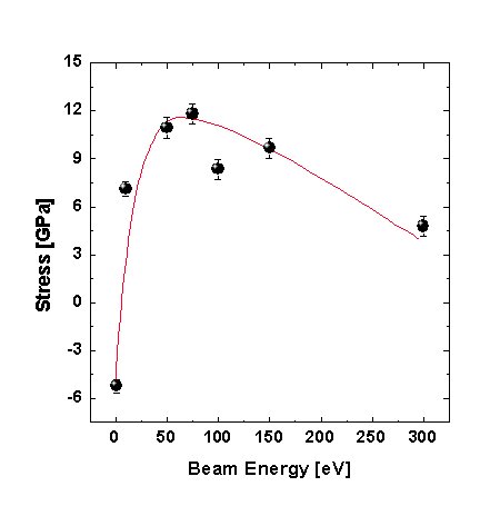
MD Simulation of a-C Atomic scale structure and the properties of amorphous carbon film was simulated by the molecular dynamic simulation using Tersoff interatomic potential for carbon atoms. Simulation results are qualitatively consistent with those of ta-C film deposited by filtered vacuum arc process. At an optimum kinetic energy of the deposited carbon atom (about 75eV), maxima in sp3 hybridized bond and the resiudal compressive stress are observed. (2003. 6. 21) |
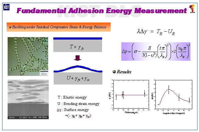
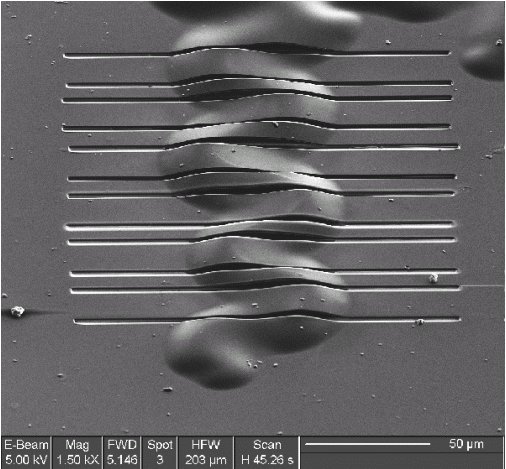
Telephone Cord Buckling When a compressively stressed film delaminates from substrate, it shows an interesting sinusoidal configuation that is also called telephone cord buckling. We are investigating the details of the buckling behaviors in both experimental and theoretical methods. Left figure is our microstructure appeared on the cover page of a book written by Prof. Freund and Prof. Suresh. Right figure is the FEM simulation result of the telephone cord buckling. (2004. 1. 18) |
||
|
|
|||
|
|
|
|
|
|
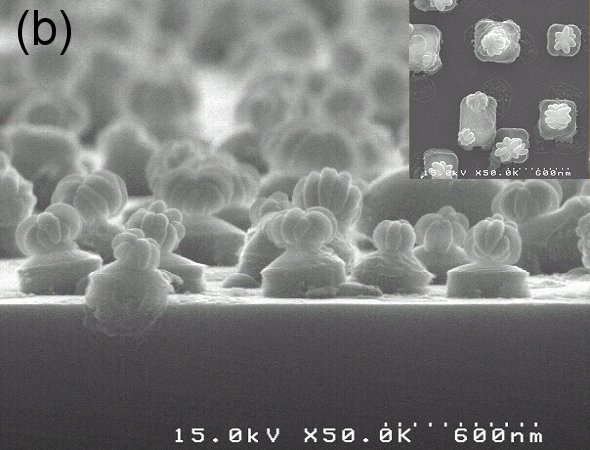
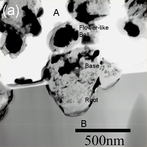
Nanoflower of Cu-Si Composite When annealing Si (100) wafer with Cu thin film on the surface at 1073K, interaction bewteen Cu and Si resulted in a fascinating microstructure of flower-like Cu-Si composite ball on the base (left). The base has an orientation relationship with the Si wafer as shown in the inset of the left figure. TEM cross section revealed that the ball is composed of Cu riched central region and Si oxide layer on the surface. (2003. 6. 21) |
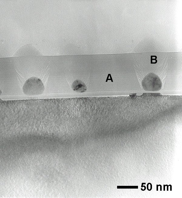
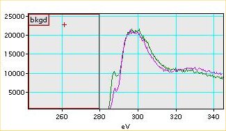
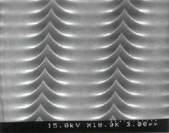
Nanoscale Structural Manipulation of ta-C Films We demonstrated a novel method to obtain a nano-composite film where nano-scale columns of graphitic phase are embedded in a tetrahedral amorphous carbon matrix. When using a Si substrate with nano-sized Ni dots on the surface, graphitic columns (indicated by B) grew selectively on the Ni dots, while a dense ta-C film (indicated by A) was deposited on the bare Si surface. TEM EELS was employed to characterize the structural difference. (2003. 6. 21)
|
||
|
|
|||
|
|
|
|
|
|
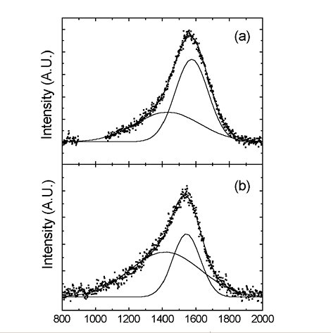
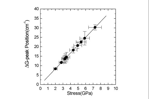
Stress Effect on the Raman Spectrum Analysis Using free overhang method which was employed to measure the elastic modulus of DLC films, we could measure the residual stress effect on the G-peak position of ta-C films. Left figure show the deconvolution result of the Raman spectra of stressed (upper) and stress relaxed ta-C films (lower). We found that the G-peak shifted upward by 4.1cm-1 per GPa of compressive residual stress (right). For more details, please refer to our publication. (2001. 5. 23). |
DLC Coated Cardiovascular Implants We are pursuing medical applications of DLC films. With researchers at MDMI Co. Ltd in Vancouver, Canada, we are developing DLC coating technology for stent. Enjoy the movie of ballooning (left figure). Our technical concerns are the adhesion of film, bio-compatibility, functionalization of the coating, and the surface coverage before and after ballooning. (2003. 5. 22) |
||
|
|
|||
|
|
|
|
|
|
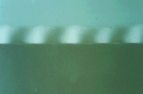
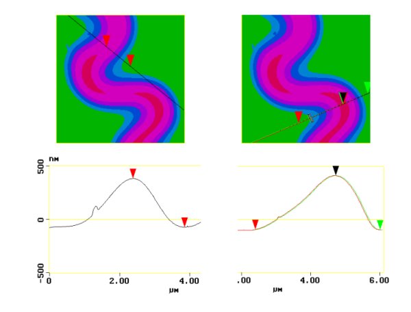
AFM Analysis of Buckled Thin Film (DLC on Glass) Details of sinusoidal buckling observed in DLC/glass system is being analyzed by AFM and FIB (Focused Ion Beam). Left figure shows the AFM image of the sinusoidla buckling. Different shape of buckling was found depending on the location in the buckling (right). This work was done by Mr. Myoung-Woon Moon with guidance of Prof. A. Evans at Pinceton University. (2001. 5. 23) |
Seectioning of Buckled DLC Film by FIB In order to analyze the details of DLC film buckling on glass substrate, focused ion beam (FIB) was used to cut the buckling region. (2001. 7. 2). |
||
|
|
|||
|
|
|
|
|
|
SEM Surface Morphology of ta-C Films Small particles of diamter about 1mm was frequently observed on ta-C film surface when using new graphite cathode (left). Surface of ta-C film coated by used cathode is much cleaner (right). The reason for this difference should be clarified for a specific application.(2000. 11.28) |
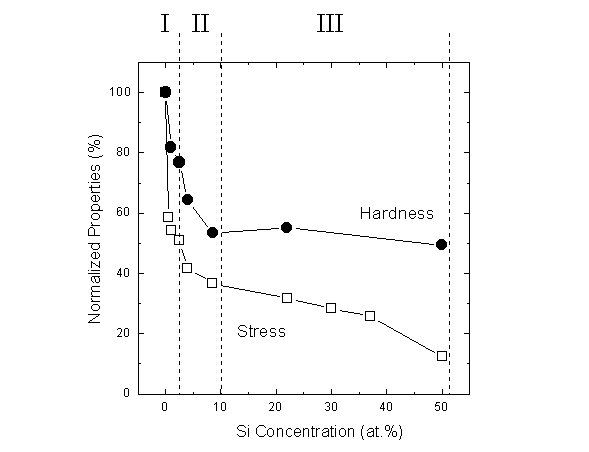
Si Incorporated ta-C films Si incorporation to ta-C films was successfully obtained by using hybrid FVA and magnetron sputterin system. Si concentration could be systematically controlled by changing Ar gas flow to the sputter gun (left). The changes in the mechanical properties occurred only when the Si concentration was less than 1 at.% (right). For more details, please refer to our publication. (2001. 5. 23) |
||
|
|
|||
|
|
|
|
|
|
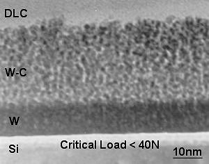
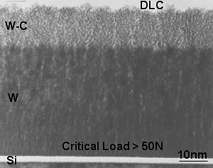
TEM Cross Section of DLC Coated Si with W & W-C Interlayer Structural continuity between W and W-C mixed layer is important for the adhesion improvement. |
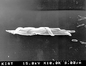
Morphology of Wear Debris Debris formation and it's behavior is a key factor to understand the tribological performance of DLC films in various test environments. |
||
|
|
|||
|
|
|
|
|
|
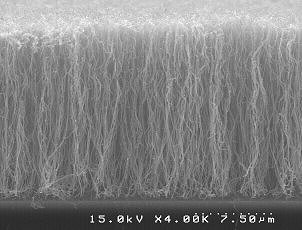
Carbon Nanotube (CNT) by Thermal CVD Vertically aligned carbon nanotube can be grown by thermal CVD method in ammonia environment.
|
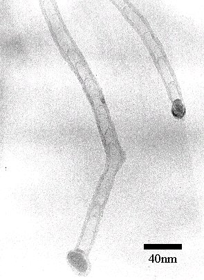
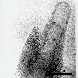
TEM Microstructure of Carbon Nanotube TEM microstructures illustrate the mechanism of the CNT growth. Bamboo growth occurs in thermal CVD with Ni catalyst.
|
||
|
|
|||
|
|
|
|
|
|
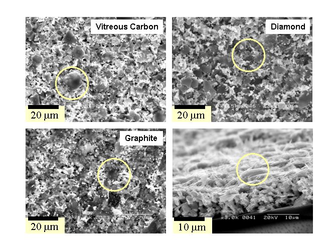
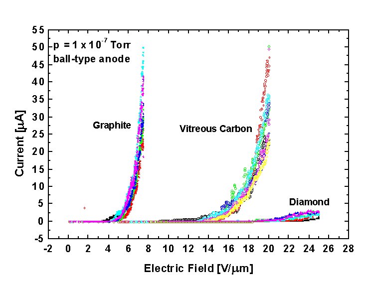
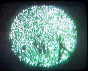
Comparison of Field Emission Behavior from Three Kinds of Carbon Materials Field emission behavior of graphite, vitreous carbon and diamond were compared to find the best carbon materials for electron emission cathode. For a reasonable comparison, powders of the same size were pasted on the same electrode. Surprisingly, graphite is the best material for the electron field emission. (2001. 5. 25) |
Field Emission from Vitreous Carbon Excellent emission behavior from vitreous carbon shows that the electron emission is not directly related to the sp3 hybridized bond of carbon.
|
||
|
|
|||
|
|
|
|
|
|
Triode of Cold Cathode using DLC as Parting Layer Triode type Si cold cathode was fabricated by using DLC film as the parting layer. |
DLC Coated Si Tip for Cold Cathode DLC overcoating on Si tip stabilized the emission behavior of Si tip. |
||
|
|
|||
|
|
|
|
|
|
Elastic Modulus of Very Thin DLC Films The free overhang method enables us to measure the elastic modlus of very thin films without considering the substrate effect. The method were employed to a-C:H (left) and ta-C (right) films. We found that the structural evolution occurs during initial stage of deposition. The structural evolution is much significant when the characteristic of DLC films were both polymeric or graphtic. [related publication] (2001. 5. 25) |
Delamination Morphology of DLC Film on Glass Sinusoidal pattern of the buckling delamination can be used to estimate the elastic properties and adhesion energy of the film.[related publication]
|
||
|
|
|||
|
|
|
|
|
|
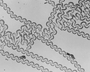
DLC Bridge by Microfabrication Technology Using high residual compressive stress of DLC film, biaxial elastic modulus could be measured by the strain of the film which can be obtained from the shape of this bridge. [related publication] |
DLC Freehang by Substrate Etching Technique This simple method can be used to measure the elastic modulus of extremely thin DLC films.[related publication] |
||
|
|
|||
|
|
|
|
|
|
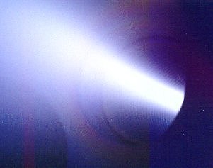
FVA Plasma Beam High ionization rate and ion energy of FVA plasma results in out- standing properties of the ta-C films. |
AFM Image of ta-C Surface on Si Smooth surface of the coating is an important advantage of DLC film.
|
ta-C as Protective Layer of HDD For very high storage density HDD, the protective layer should be thinner than 5nm. ta-C film of excellent mechanical properties is a strong candidate for the purpose. |
|
|
|
|||
|
Last Update : 2007.6.15 |
|
|
|
.jpg)
-110.jpg)
-100.jpg)


.jpg)
.jpg)

.jpg)


.jpg)
.jpg)